


Integrated circuits (ICs), commonly known as microchips, are tiny electronic circuits etched onto semiconducting material. They hold hundreds to billions of transistors, resistors, and other components in a small package. These microchips form the backbone of nearly every modern electronic device, from computers and smartphones to cars and appliances.
Understanding the history of integrated circuits reveals how a succession of innovations – from vacuum tubes and early transistors to modern planar processing and photolithography – enabled today’s IC technology. It also highlights the invention of the integrated circuit and the rapid IC development that followed. In the broad sweep of semiconductor history, ICs stand as one of the most transformative inventions, alongside the transistor.
In this blog post, we will trace the timeline of IC technology evolution and microchip invention from its earliest roots to the present day. We will cover how engineers like Jack Kilby and Robert Noyce sparked the first integrated circuits in 1958–59, and how manufacturing processes (IC fabrication) grew to deliver billions of transistors on a single chip. Along the way, ideas like Moore’s Law will show how IC development accelerated, paving the way for our modern digital age.
Table of Contents
Early Electronics: Vacuum Tubes, Transistors, and the Need for Integration
Before integrated circuits, electronic devices used vacuum tubes. These glass tubes could switch and amplify electrical signals, but they were bulky, power-hungry, and unreliable. Early computers like the ENIAC (1945) contained thousands of vacuum tubes, weighed tons, and consumed enormous power. By the late 1940s, a new technology replaced tubes: the semiconductor transistor. In 1947 at Bell Labs, John Bardeen, Walter Brattain, and William Shockley built the first working transistor. Transistors were smaller, faster, and far more reliable than vacuum tubes. They quickly replaced tubes in most electronic equipment.
However, as transistors made circuits more compact, engineers ran into the “tyranny of numbers.” Each electronic board still required dozens of discrete transistors, resistors, and capacitors, each wired by hand. Complex systems needed hundreds or thousands of wires, making assembly error-prone and time-consuming. Any loose connection could break the entire circuit. This motivated engineers to think bigger: what if many components could be integrated into one piece of semiconductor, with the connections also built in? In other words, if many transistors and other circuit elements could be built together on one chip, it could eliminate most of the tedious wiring.
- Advantages of integration: Combining parts on a single chip promised huge benefits. Integrated circuits would drastically shrink the size and weight of electronic systems. They would eliminate most manual wiring, improving reliability and assembly speed. Signals in an IC travel shorter distances, boosting speed and lowering power consumption. Mass-produced chips also cut costs compared to hand-made discrete circuits.
Imagining the Microchip: Early Integration Concepts (1949–1957)
The idea of a microchip did not emerge overnight. In 1949, German engineer Werner Jacobi (Siemens) filed a patent for an “integrated amplifier” – an early vision of multiple transistors on one semiconductor substrate. Jacobi’s design envisioned five transistors and resistors on a single piece of semiconductor, acting as a multi-stage amplifier. Although it never became a commercial product, it showed the potential of placing multiple active elements together.
A few years later, in 1952, British engineer Geoffrey Dummer proposed a similar concept. Working on radar electronics, Dummer sketched a monolithic circuit idea at a symposium: many components could be built in one block of material to avoid the wiring problem. He even attempted to build such a circuit around 1956, but the technology was not yet mature (for example, there was no proven way to isolate individual devices or pattern tiny parts on a chip). Other pioneers like Sidney Darlington and Yasuo Tarui also explored integrating circuits by sharing active silicon regions among components.
The common insight was that silicon or germanium wafers might host entire circuits. Yet key challenges – how to isolate components and how to connect them on a tiny chip – remained unsolved. Still, these early concepts set the stage for the microchip invention by showing that integrated electronics were theoretically possible. Engineers realized that if they could master semiconductor processing and interconnect techniques, the integrated circuit could solve the wiring nightmare.
Jack Kilby and the First Integrated Circuit (1958)
The first breakthrough came in 1958 at Texas Instruments. Jack Kilby, a young engineer there, conceived a radical solution: build an entire circuit from one block of semiconductor. In July 1958 he recorded his idea of a “monolithic” chip and began experimenting. By August 1958, Kilby had built the world’s first working integrated circuit. It was a small piece of germanium containing one transistor, two resistors, and one capacitor, with fine gold wires on top connecting these elements. When he powered it up in September 1958, the circuit worked exactly as intended.
Kilby quickly realized the importance of his prototype and filed a patent application in early 1959. He described a “body of semiconductor material… wherein all the components of the electronic circuit are completely integrated.” The U.S. Air Force became the first customer for this new chip, recognizing its potential for military electronics. Decades later, Jack Kilby would be awarded the Nobel Prize in Physics for this invention.
It is worth noting, however, that Kilby’s 1958 IC had limitations. It was made of germanium (rather than silicon) and still required some manual wire-bonding for connections. Mass-producing such chips would be challenging. Nonetheless, Kilby’s prototype was the first integrated circuit, proving the concept. He demonstrated that making an entire circuit on one piece of material was possible. As Kilby later said, solving the wiring problem by integrating all components was the key to making electronics smaller and more reliable. His microchip invention sparked a revolution in electronics.
Robert Noyce and the Planar Silicon Chip (1959)
Within a year, another engineer refined Kilby’s idea and made integrated circuits truly practical. In late 1959, Robert Noyce at Fairchild Semiconductor applied new silicon fabrication techniques to IC design. Silicon itself was crucial: by the mid-1950s, silicon had overtaken germanium for transistors because it could operate at higher temperatures and with greater stability. (In 1954, TI had produced the first silicon transistor.) In 1959, Fairchild engineer Jean Hoerni developed the planar process, a method to form flat silicon dioxide layers on a wafer and use photolithography to create transistor structures.
Noyce’s genius was to combine this with on-chip wiring. He took a silicon wafer with transistors formed by Hoerni’s process and then deposited a thin layer of aluminum over it. By etching patterns into this aluminum layer, he created all the wires connecting the transistors and other components on the chip itself. In other words, Noyce put the circuit connections on the same silicon die instead of using external wires. By mid-1960, he had built a working planar silicon IC at Fairchild.
Fairchild filed a patent for Noyce’s silicon planar IC in late 1961 (granted in 1964). This patent became the blueprint for modern ICs. Robert Noyce later co-founded Intel, where he continued to advance integrated circuit technology. In retrospect, Noyce’s design – silicon-based, planar, with built-in metal interconnects – is the model used by virtually every semiconductor today. It solved the manufacturing problems of Kilby’s IC and made large-scale production possible.
At roughly the same time, engineer Kurt Lehovec at Bell Labs invented a key technique called p–n junction isolation, which helped keep adjacent transistors electrically separate on the same chip. Together, Hoerni’s planar process, Lehovec’s isolation, Kilby’s idea, and Noyce’s wiring completed the semiconductor history of IC invention. By 1960, the basic integrated circuit was fully realized, and the path was open to commercial production.
IC Fabrication: The Planar Process and Photolithography
Once the IC concept was established, the focus shifted to manufacturing. The foundation was the planar fabrication process. This method builds circuits layer by layer on a flat silicon wafer. The process begins with a polished silicon wafer. A thin insulating layer of silicon dioxide is grown on its surface. Then photolithography comes into play: engineers coat the wafer with light-sensitive photoresist, align a patterned mask over it, and shine ultraviolet light through the mask. This transfers the pattern onto the wafer, exposing select areas.
After exposure, the wafer undergoes chemical processing. Where the photoresist was exposed, the silicon dioxide might be etched away, exposing the underlying silicon. In those exposed regions, dopants (impurities like phosphorus or boron) are introduced into the silicon by diffusion or ion implantation. This “doping” changes the electrical type of the silicon, creating the transistor’s source, drain, and base (or well) regions. Each mask step can form different parts of the transistor or other components.
Once the silicon devices are formed, another photolithography step is used to pattern the metal interconnect. A thin film of metal (originally aluminum, later copper) is deposited over the wafer and then etched to leave wires connecting the transistors. Multiple metal layers can be added by repeating mask-and-etch steps with insulating layers (often silicon dioxide) in between, enabling very dense multi-level wiring.
Because photolithography allows printing many chips on a wafer at once, planar fabrication is highly scalable. Crucially, advances in lithography allowed features to shrink dramatically over time. For instance, early 1970s ICs had feature sizes around 10 micrometers. By the 1990s, chips were using 100-nanometer features (0.1 micrometer). By the 2010s, production nodes reached tens of nanometers. Each generation of smaller features meant more transistors fit on the same chip area. This shrinking followed Moore’s Law for decades.
- Modern chip fabs: Today’s semiconductor fabrication plants use extreme ultraviolet (EUV) lithography to etch features as small as 3–5 nanometers. A modern processor may have over a dozen layers of metal interconnect. Once a wafer is fully processed, it is diced into individual chips (dies), each tested and packaged into standard housings for circuit boards. Although the process can take many weeks for a leading-edge chip, automation and quality control yield a high percentage of functional microchips.
In summary, IC fabrication relies on the planar process and photolithography invented in the late 1950s. These techniques turned integrated circuits from lab curiosities into mass-produced devices. As lithography and etching techniques improved, chip sizes decreased and transistor counts skyrocketed.
Commercialization and the Space Race (1960s)
With fabrication techniques in place, companies began turning ICs into products. Around 1960–1961, Fairchild, TI, and others started producing simple IC components like diodes, transistors, and basic logic gates. Texas Instruments announced the SN502 flip-flop (a 6-transistor IC) as one of the first commercial integrated circuits. Early sales were modest, partly because yields were low and customers were cautious. A major push, however, came from defense and space programs.
In 1961, Texas Instruments delivered one of the first fully IC-based computers to the U.S. Air Force. This experimental solid-state computer occupied only 6.3 cubic inches and weighed 10 ounces (about the size of a deck of cards) – yet it performed the same functions as an earlier system that was 150 times larger. Astonishingly, the IC computer used only about 587 on-chip transistor circuits, while the conventional design used around 8,500 discrete components. This demonstration dramatically showcased the miniaturization that integrated circuits could achieve.
Soon after, NASA’s Apollo program became the largest early customer of ICs. When President Kennedy announced the Moon landing goal, NASA needed compact, reliable computers for guidance. In 1961, NASA awarded MIT’s Draper Lab the contract to build the Apollo Guidance Computer (AGC) and specified ICs for much of its circuitry. Fairchild, Raytheon, and other companies manufactured custom silicon IC logic chips for the AGC. By the mid-1960s, NASA was purchasing thousands of these chips for spacecraft. The success of Apollo – with its IC-based computers – proved the reliability of silicon chips in demanding environments.
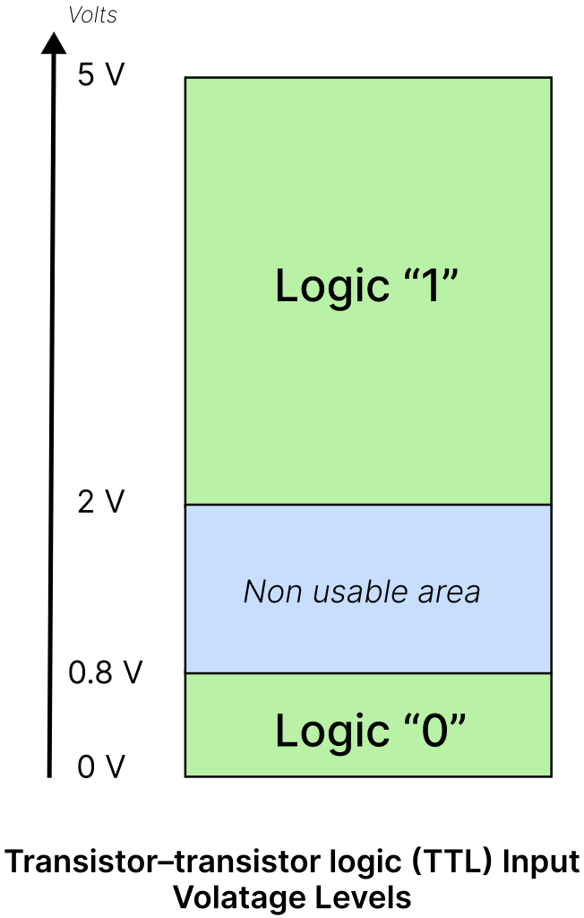
Integrated circuits also began entering commercial electronics in the 1960s. Mainframe and minicomputers from IBM, DEC, and others adopted ICs on their circuit boards. In 1963, engineer James Buie of TRW invented TTL (Transistor-Transistor Logic), a fast digital IC family. TTL chips and related logic families (like ECL – Emitter-Coupled Logic) became standard building blocks for digital computers and communications. Circuits with a few gates per chip (small-scale integration, SSI) gave way to chips with dozens of gates (medium-scale, MSI) as the decade progressed.
Key Milestones in the 1960s
- 1961: TI delivers an IC-based computer (6.3 in³, 10 oz) to the U.S. Air Force, replacing a much larger system.
- 1961: NASA contracts MIT’s Draper Lab to build the Apollo Guidance Computer, which will rely heavily on ICs.
- 1963: Invention of TTL (Transistor-Transistor Logic) by James Buie, setting a new standard for digital ICs.
- 1965: Gordon Moore formulates Moore’s Law, observing that IC components double roughly every year (later revised to two years).
- 1969: Apollo 11 lands on the Moon using an IC-based guidance computer, proving the reliability of microchips in space.
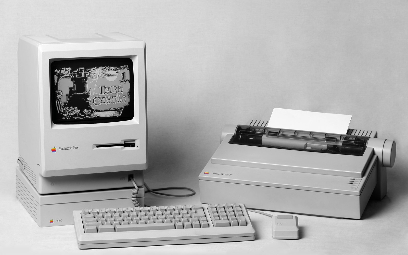
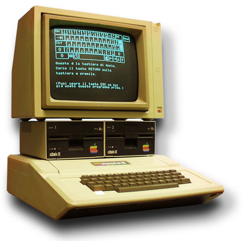
By 1970, integrated circuits had moved beyond prototypes into real products. The semiconductor industry expanded quickly: new companies (like Intel and AMD) entered the field, and existing firms scaled up chip production. Standard packages, such as the plastic dual-inline package (DIP), made it easy to incorporate ICs on circuit boards. Large-scale integration (chips with hundreds of transistors) became practical. This set the stage for the next era: squeezing an entire computer’s logic into a single chip.
Moore’s Law and the Microprocessor Revolution (1970s–1980s)
As ICs proliferated, Gordon Moore’s prediction held true. From the late 1950s through the 1970s, the number of transistors per chip roughly doubled every year, and later about every two years. Each new fabrication generation shrank transistors and expanded the chip’s functionality. Thanks to Moore’s Law, ICs became dramatically more powerful and cost-effective over time.
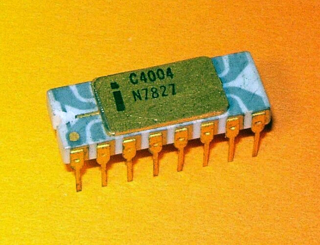
A major catalyst in this era was the microprocessor – a CPU on one chip. In 1971, Intel introduced the 4004, the first commercial single-chip microprocessor (about 2,300 transistors). Initially designed for calculators, the 4004 showed that an entire arithmetic unit could fit on a tiny chip. In 1974, Intel followed with the 8080 (about 6,000 transistors), an 8-bit CPU used in early personal computers. These inventions put whole computer brains on chips and fueled the personal computing revolution.
Memory chips also advanced rapidly. In 1970 Intel released the 1103, the first commercial DRAM chip, making semiconductor memory the new standard (replacing magnetic core memory). Over the 1970s and 1980s, DRAM and ROM capacities climbed from a few kilobits to megabits as feature sizes shrank. This meant computers could store vastly more data in silicon memory on each board.
By the mid-1980s, microprocessors and other ICs contained hundreds of thousands of transistors. For example, Intel’s 80386 CPU (introduced 1985) had about 275,000 transistors; by 1989 the 80486 had over a million. Memory and specialized chips likewise grew in density. Engineers continued to improve designs (for instance, adopting silicon-gate technology and CMOS logic) to boost performance and reduce power. Throughout these decades, miniaturization followed Moore’s Law: each new generation of chips delivered roughly twice the logic and memory at a similar cost, enabling faster computers and cheaper electronics.
In summary, the 1970s–80s were a golden age of IC innovation. The invention of the microprocessor put the power of a computer on a chip. Large-scale integration (LSI) became very-large-scale (VLSI) with tens of thousands of transistors per die. As a result, computing power exploded: a modern home computer had more capabilities than a room full of 1970s mainframes. Integrated circuit technology evolution in this period laid the foundation for the digital world that followed.
The PC and Mobile Era: VLSI to Nanometer Technology (1990s–Present)
By the 1990s, integrated circuits had entered the ultra-large-scale integration era. Chips with millions of transistors were common. Personal computers, which had appeared in the 1980s, now relied on advanced ICs: for example, Intel’s Pentium processor (introduced 1993) contained over 3 million transistors. As computing spread to laptops and mobile devices, chips continued to get smaller and more capable.
Key developments in this period included:
- CMOS technology: CMOS (complementary MOS) became the dominant process for most ICs, including logic and memory. It offered much lower power use than earlier bipolar circuits, enabling battery-powered devices and smartphones.
- Multi-core processors: In the 2000s, designers put multiple CPU cores on a single chip to improve performance. Today, desktop and smartphone processors often have 4, 8 or more cores, all integrated in one package. GPUs (graphics chips) also grew massively in cores for parallel tasks.
- System-on-Chip (SoC): Especially in smartphones and IoT devices, entire systems (CPU cores, GPUs, memory controllers, radios, etc.) are integrated onto one silicon chip. These SoCs contain billions of transistors and handle everything from computing to communication on a single die.
- Memory scaling: DRAM and flash memory chips continued their own evolution. Early 1980s DRAM chips held kilobytes, while by the 2000s they held gigabits. NAND flash memory emerged for storage. This memory scaling meant that gigabytes of RAM and storage could sit on a few chips in a desktop or mobile device.
Simultaneously, fabrication technology marched forward. Feature sizes dropped from hundreds of nanometers in the 1990s to tens of nanometers by the 2010s. For instance, the industry progressed from 250 nm nodes (mid-90s) down to 180 nm, 130 nm, 90 nm, 65 nm, 45 nm, and so on. By 2020, leading-edge processes reached 5 nm and 3 nm, allowing tens of billions of transistors on a single chip. Each shrink roughly doubled transistor density.
Packaging technology also evolved. Chips moved from through-hole DIP packages to flat chips with hundreds of pins. Ball grid array (BGA) and flip-chip packages became common, enabling higher pin counts and better heat dissipation. 3D stacking (like stacking memory dies) began to appear in high-end products.
The net effect is staggering: by following Moore’s Law for decades, the semiconductor industry made computer power routine. A modern smartphone is millions of times more powerful than 1980s computers. At the same time, prices dropped and energy efficiency improved. Integrated circuit development in the 1990s–2000s turned computing from a niche activity into an everyday utility.
Modern Integrated Circuits: Nanotechnology and Beyond
Today’s chips exist at the cutting edge of nanotechnology. Feature sizes are measured in nanometers (nm), one-billionth of a meter. Leading-edge fabs now pattern features as small as 3–5 nm. At these scales, a single chip can contain well over ten billion transistors. For example, modern GPU or AI chips may pack 30–50 billion transistors.
Reaching these tiny dimensions has required new innovations. Traditional flat transistors have been replaced by 3D structures. The industry moved from planar FETs to FinFETs (fin-shaped transistors) in the 2010s, and now to Gate-All-Around transistors for even better control at nanoscale. New materials (like silicon-germanium channels and high-k dielectrics) were introduced to sustain performance. Engineers also use extreme ultraviolet lithography (EUV) to print finer details.
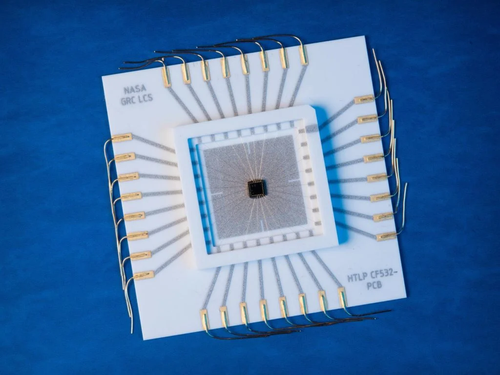
Beyond silicon, researchers are exploring new technologies. Carbon nanotube transistors, graphene interconnects, and other novel devices have been demonstrated in labs. Photonic (optical) interconnects on chips aim to send data with light instead of electrons. Some companies are even experimenting with specialized chips for quantum computing (where information is stored in qubits, not traditional transistors).
Meanwhile, 3D integration has become common. Memory chips (like 3D NAND flash) stack dozens of silicon layers to boost capacity. Some systems use stacked “chiplets” or through-silicon vias (TSVs) to pack more transistors into a volume. These approaches effectively add computing power without further shrinking planar feature size.
In summary, while Moore’s Law scaling is slowing, integrated circuit technology continues to evolve. The current frontier combines nanoscale silicon with novel architectures (multicore, AI accelerators, neuromorphic designs) and 3D structures. Even as we approach physical limits, the history of ICs suggests new breakthroughs will keep the progress going.
Integrated Circuits Today: Impact and Applications
Integrated circuits are now everywhere. Every personal computer and smartphone relies on dozens of ICs: CPUs, graphics chips, RAM and flash storage chips, power management units, wireless radios, and more. But ICs are not limited to computing gadgets. Today’s automobiles have dozens of microcontrollers overseeing engines, safety systems, infotainment, and driver-assist features. Home appliances – from smart TVs and refrigerators to thermostats and light bulbs – contain chips to add intelligence and connectivity.
Data centers and communication networks run on custom ICs. Servers use thousands of multicore CPUs and GPUs. Networking gear (routers, switches, cell towers) relies on specialized ASICs and FPGAs. Even medical devices (MRI machines, imaging systems) and industrial robots depend on reliable microchips. The sheer scale of IC use is breathtaking: estimates suggest more than 100 billion microchips are produced every year for all purposes combined.
One of the biggest trends is the Internet of Things (IoT). IoT envisions billions of smart sensors and devices – wearable trackers, smart home gadgets, environmental sensors, etc. – all connected to the internet. Each of these devices uses a tiny low-power microcontroller or SoC. For example, a smart light bulb might contain a few simple ICs (a microcontroller, a wireless radio, some memory) for under a dollar cost. These chips often run on very low power, showing how far IC development has come to support battery-powered applications.
Integrated circuits have also revolutionized areas like artificial intelligence. Modern AI algorithms rely on huge amounts of computation. Graphics Processing Units (GPUs) and AI accelerators are specialized ICs with many parallel cores (billions of transistors) designed for matrix math. Companies like NVIDIA, Google, and others have built chips specifically for neural networks. The performance of these AI chips – measured in teraflops or more – would have been unthinkable without decades of IC scaling.
In short, the integrated circuit permeates every aspect of modern life. It made the personal computer and smartphone possible. It enabled the internet and the digital economy. It brought powerful computing into cars, homes, and even our pockets. When we look at any modern technology, it’s almost certain that dozens or hundreds of ICs are at work inside it. From the earliest microscopes to today’s laptops, the story is the same: smaller, faster, cheaper chips changed everything.
The Future of Integrated Circuit Technology
Looking ahead, the core drivers of IC evolution remain: more transistors, higher speed, and lower cost. Engineers and scientists are already pursuing the next frontiers. One path is continuing to shrink transistors with new materials and 3D designs, squeezing more power into each chip. Another path is specialty architectures: for example, chips designed for quantum computing or brain-inspired neuromorphic computing.
3D integration will also grow. Stacked chip layers (beyond just memory) and chiplet architectures let designers mix different technologies in one package. This can overcome the limits of monolithic scaling. Power efficiency is another focus: low-power “ultrascale” ICs and energy-harvesting chips will enable new IoT devices and wearables. Research into novel devices (like memristors or single-electron transistors) could eventually replace or augment conventional CMOS transistors.
Governments and industries worldwide recognize the importance of continuing IC innovation. Initiatives like the U.S. CHIPS Act and similar programs in Europe and Asia are funding next-generation semiconductor research and fabrication. Foundries now use extreme ultraviolet lithography and are developing 2 nm processes and beyond. These efforts aim to sustain the spirit of Moore’s Law even as we approach atomic scales.
Conclusion: From its beginnings in 1958 with Jack Kilby’s germanium chip and Robert Noyce’s planar silicon chip, the integrated circuit has transformed technology and society. Moore’s Law captured the astonishing growth in IC capability, and decades of IC development have delivered billions of transistors on a single chip. Today’s billion-transistor microchips enable smartphones, cloud computing, artificial intelligence, and much more. The history of the integrated circuit is the history of modern electronics. As we look to the future, each new breakthrough in IC technology will build on this legacy, driving the next wave of innovation in the digital age.